
Assignment 1.3: Technical Definitions
In this first Assignment, the task was to define a technical word to a non-technical audience using three different techniques. The definition was to be accompanied by a simple scenario, and an introduction of the assignment task. I chose the word “bandstructure” and provided an explanation as to how bandstructure allows one to characterize materials as metals, semiconductors, or conductors.
Introduction
The purpose of this assignment is to not only appreciate the need for technical definitions, but to understand the necessity of considering a non-technical audience when defining complex terms. The assignment itself will have 3 parts:
- to choose a complex technical term relating to my professional field
- to create a hypothetical situation and an audience of non-technical readers for which we will write to explaining our technical term
- create a definition for our technical term using three different defining techniques:
-
-
- via a parenthetical definition
- via a sentence definition
- via an expanded definition
-
The expanded definition should contain 4 different expansion strategies as listed in Technical Communication: 14th Edition, as well as at least one visual, and no fewer than three outside references (cited in MLA or APA style). The expansion strategies that I used are: operating principle, analysis of parts, comparison and contrast, examples, and visuals. The parenthetical definition is included in the first sentence, while the sentence definition is the second sentence, and the definition continues as an expanded definition.
Technical Terms and Definitions
Technical Term: Band structure
Situation: Dr. Alana Ginsley works as a physics professor for a first year course. While most of her students are familiar with the concept of conductors, insulators and semiconductors, she wants them to understand exactly how it is that materials can behave in different way. She is putting together an article that will define the concept of “band structure”, using simple language that requires no knowledge of quantum mechanics or solid state physics.
Audience: The intended audience, who have a high school level knowledge of physics and chemistry, are familiar with the concept of conductors and insulators, but may not know why exactly the materials behave differently. Many of these students do not intend to pursue solid state physics, so while it is important to understand band structure, the definition does not need to be entirely comprehensive.
Band Structure
Band structure (the allowed energies that electrons can potentially occupy in a material) describes how electrons can move within a certain medium. Band structure is a characteristic of materials that describes how electrons are bound to atoms and explains (among other things) whether the material can conduct electricity. To fully comprehend the significance of band structure, we first have to understand single atomic structure, and then see how electrons behave when single atoms bind to form a material.
Single Atom Structure
You may remember from prior courses that atoms are made up of protons, neutrons, and electrons. Elements are defined by the number of protons in their nucleus, but most stable elements will have the same number of electrons as protons. When talking about band structure, we will talk mostly of electrons. According to quantum mechanics, electrons are only allowed to exist in discrete energy states surrounding the nucleus, and only a certain number of electrons can exist in each state. Additionally, each state corresponds to a different energy, and the lowest energy states fill up with electrons first. Now, say we take many many atoms of different elements and make a solid material out of it.
Material Structure
The electrons in this material will organize themselves so they can only exist in different bands of energy. Whether this material can conduct or not has to do with the band structure of the material, and like before, the electrons fill up the lowest energy bands first. The most notable aspects of a material’s band structure is the conducting band and the valence band (see fig. 1), which is the two highest bands of energy after all the electrons have been “placed” in the different energy potentials. Strictly speaking, all bands with energy below the valence band are completely “filled” with electrons, so it is only the valence and conduction band that is most important.

Fig. 1 A valence band and conductance band where electrons could potentially reside, where the y axis is energy. (Singh, 2003)
Each material has a “fermi level” (the extent to which the electrons fill the bands at absolute zero), which can give information about the class of material. In other words, the fermi level will dictate how much energy the highest energy electron can have. The question then becomes, if every material has discrete bands of energy that electrons could POTENTIALLY live in, are these bands occupied or unoccupied by electrons? And what does this have to do about the classification of materials?
Bandstructure for Classification
Using the examples of insulators, conductors and semiconductors, we can see how the band structures will help us classify these materials as such (see fig. 2).
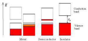
Fig. 2 Band structures of metal, insulators and semi-conductors. Where red represent electrons, E represent energy, and Eg is the difference in energy between bands. The red and white interface will represent the fermi level of the material. (Kittel, 2005)
Insulators: For insulating materials, the fermi level lies between the valence and conduction band. This means that the entire valence band is filled, and therefore cannot conduct electricity. You can compare this to a busy highway that is filled with cars transporting electricity. There’s so much traffic that none of the cars can move, and therefore no electricity is moving as well.
Conductors: Conducting materials have a fermi level that lies halfway between a band itself. This is called a “half-filled band”. Using the same analogy before, this is as if the cars transporting electricity are on a highway with plenty of room to travel, thus electricity is being transported efficiently.
Semi-conductors: Like insulators, the fermi level for semi-conductors lies in between the valence and conductance band. However, in contrast to insulating materials, the distance between the valence and conductance band is smaller. This means that electrons with a high enough energy can “jump” into the conductance band, and electricity can flow. You can think of this as if on a very busy highway, cars with high enough occupancy can enter the HOV lane, and move unencumbered by traffic.
Of course, this is a simple definition and band structures of materials can become quite complex. For your entertainment, below is a calculated bandstructure for Germanium (Ge).
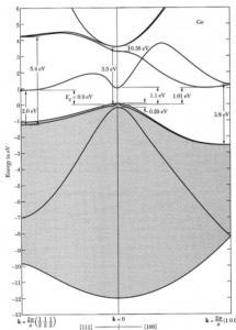
Fig. 3 Band structure of Germanium (Ge) (Zeeghbroeck, 2011)
Citations:
Kittel, Charles. Introduction to Solid State Physics (8th Edition). John Wiley & Sons, Inc., 2005.
Singh, Jasprit. Electronic and Optoelectronic Properties of Semiconductor Structures. Cambridge University Press, 2003.
Zeeghbroeck, B. Van. “Chapter 2: Semiconductor Fundamentals.” Principles of Semiconductor Devices, 2011, ecee.colorado.edu/~bart/book/book/chapter2/ch2_3.htm.