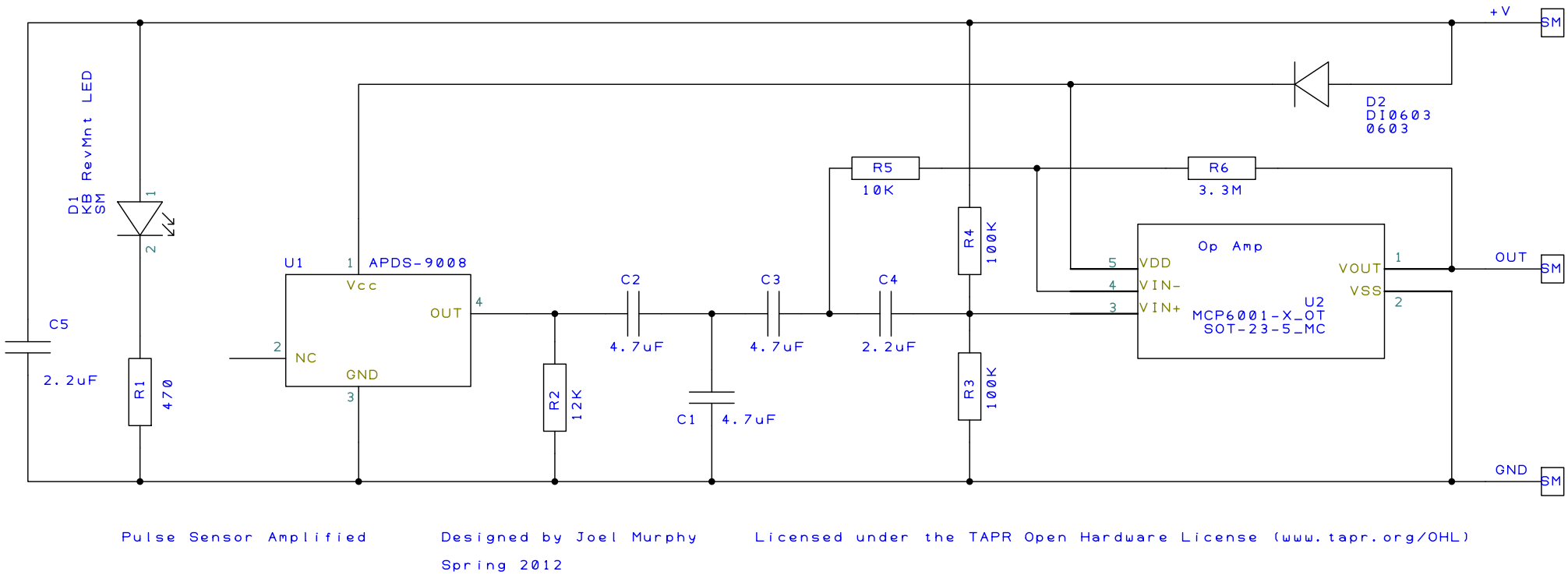
This is the current schematic of the hardware used by the open sourced pulse sensor board (credits to Joel Murphy @ www.pulsesensor.com) we are currently using. I will run through it to so as to give a brief idea of what each component does in the scope of the inputs and outputs to the system. Also, I will discuss ways to mitigate risks and problems with the board.
Inputs and Output
The inputs to the system are simply V+ (can be either 3.3V or 5V) and GND. They are used to power up the LED, the photo detector as well as the opamp. The output from the system measures the amount of light received from the photosensor after noise filtration, amplification and modulated about the baseline.
Parts of the circuit
Diode Protection The photodetector and opamp are protected by a schottky diode (D2) in case the V+ and GND are reversed.
LED driver circuit The LED D1 is forward biased and connected between V+ and GND through a 470Ohm resistor. Typical forward voltage of the LED is 3.3V, so when powered with a 5V input, the LED draws 3.6mA.
Photodetector ADPS-9008 is the photodetector model being used. Its spectral sensitivity is similar to the human eye, which means it is sensitive to RGB, but not IR. The photodetector converts the incident light into a current output which is pushed out the chip through the output pin. The light (and current) consists of a DC component (made up of light reflected from tissue and bone) and a pulsatile AC component (light reflected from blood). The output current goes from 40uA at 100lux light signal to 200uA at 500lux (almost linear response). When this current is sunk into the 12k ohm resistor, the voltage at the output pin can go up to 480mV (100lux) to 2.5V (500lux).
Signal conditioning
Concepts helpful for circuit analysis
Principal of linear superposition An input signal can be broken down into different components that together add up to it. The response of the circuit to each of these components can be analyzed separately and all the responses added up to give the response to the total input.
Impedance of capacitor The impedance(resistance to flow of current) of capacitors to different voltage signals depends on the frequency. Lower the frequency, higher the resistance of capacitance. For truly DC signals, capacitors act as infinitely high impedances similar to open circuits.
DC circuit analysis Capacitors C3 and C4 act to disconnect the circuit into two independent parts. For any constant voltage input, the output is expect to be 0.5*V+ as the capacitors decouple the two parts of the circuit.
AC circuit analysis All supply rails go to AC ground.
As mentioned previously, the resistor R2 is used a current to voltage converter, translating the current output of the photosensor into a voltage.
R5 and R6 act as a inverting gain amplifier with an eye popping gain of 330 (3.3MOhm/10KOhm). By giving the +ve terminal of the opamp a virtual ground voltage of 2.5V, the amplification is centered around 2.5V.
Current to voltage conversion The current output through the photodetector is sunk into the
Package, Fabrication and Assembly considerations
Diode In its current form, the diode is in an 0603 package and hence leading to loss of yield during assembly. To avoid this, this package will have to probably be modified to a SOT or SOD package.
LED The LED is a reverse mount Z bend LED that can be mounted on the component side of the PCB but still emits light towards the other side through a through hole drilled in. Alignment and orientation of the LED light with the through hole is mediated by the surface tension of molten solder pulling it into a symmetrical position. Hence, the tCream layer dimensioning is critical for output signal. The positioning can also be corrected using a smaller drill hole ensuring a snug fit. The current version of the PCB has a higher prescribed tolerance so as to get the LED into the hole in the first place. Now that this has been confirmed, the tolerance can be reduced.
Addnl. notes When the LED is viewed from the back, the smaller metal bit in the die goes to the higher voltage.