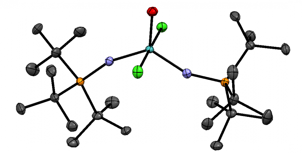
Transistors are a piece of technology universally used in modern devices today, and a smartphone in your pocket will contain about two billion. Transistors are used to amplify electronic signals and switch them on and off, and are the reason for the sophisticated technology we have access to. They are semiconductors, meaning they conduct electricity worse than a metal but better than a resistor, and commonly made of silicon or germanium.
A diagram showing the energy difference an electron needs to overcome for movement in a metal, semiconductor, and resistor.
A basic transistor. Source: Wikimedia Commons
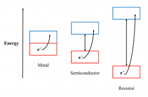
However, there is a limit to the size of a transistor, one that we grow ever closer to. This has prompted research into quantum technology, designing new devices with new components that have exponentially faster computing speeds than our current technology. Rather than semiconductors, quantum devices use superconductors, materials with zero electrical resistance when cooled below a certain temperature.
A quantum computer developed by IBM. Source: Flickr
Some researchers have considered a new design to develop more advanced computing: a hybrid semi/superconducting transistor. Yan et al. published a study describing a new method of producing these in March of 2018. They took advantage of epitaxial semiconductor crystal growth, meaning highly ordered growth, on top of a crystalline superconductor to achieve this. This allowed for the production of a semiconducting transistor on top of a superconductor. Here is a video simulating some different forms of epitaxial growth that show its very consistent order:
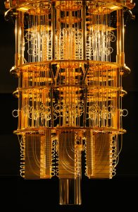
This new transistor design has the potential to be used as a superconductor or semiconductor at will, only requiring a temperature change to activate or deactivate superconductivity. As well, Yan et al. achieved this using nitride based semiconductors and superconductors, which are non-toxic and very stable, presenting some interesting applications. This differs from many common arsenic-containing semiconductors, like indium arsenide, that are quite toxic. They also found that the produced transistor had a property called negative differential resistance (NDR) when superconductive, which allows for amplification of electric signals. Telephone lines use this property, and the ability of the transistor to activate or deactivate NDR with temperature has potential use.
A Gallium Nitride crystal, the semiconductor Yan et al. used. Source: Wikimedia Commons
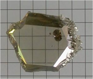
While Yan et al.’s method shows promise for the future, there were some significant issues in their specific method. The most relevant was that they found fairly low electron mobility in their material, something that another semiconductor like indium arsenide excels in. This presents one of the biggest limitations of this current design, as matching the mobility of indium arsenide will be difficult.

Indium Arsenide, a highly effective yet toxic semiconductor. Source: Wikimedia Commons
While Yan et al.’s specific design may not be the solution to transistor limitations, it does present a promising method for designing a different hybrid transistor. Hopefully, other researchers can use this result to produce an even more effective transistor so that widespread quantum computing can become a reality. If you would like a more scientific summary of Yan et al.’s paper, you can find it here, published by the Nature journal.
– Nicholas Patterson