
“It can’t go on forever. The nature of exponentials is that you push them out and eventually disaster happens”
This stark comment made in 2005 by Gordon E. Moore, a co-founder of Intel, has served as a wakeup call for computer scientists who have known for nearly forty years that mainstream manufacturing processes for computer circuitry will soon become obsolete.
Ever since its original conception in 1965, Moore’s Law has predicted that roughly every two years, the number of transistors put into a computers central processing unit (CPU) will double. Moreover, each time the amount of transistors doubles, Why should you care about this trend? First, progress in the development of the increasingly intelligent technologies that effect our lives relies heavily on this trend. Insofar as over time, we depend on our computers becoming faster, while simultaneously staying cool, small and economic to operate; so that we can innovate with them.

Much of human progress, from consumer electronics to medical breakthroughs, relies on the Moore’s Law continuing for the foreseeable future. Credit: Ray Kurzweil and Kurzweil Technologies, Inc. (Wikimedia Commons)
Second, Intel has predicted that as soon as 2021, new strategies for designing computer hardware will need to be implemented or development of exciting new technologies will be stunted dramatically. Consequently, computer scientists have been researching the future of manufacturing the CPU, and the prospects are encouraging.

An electro-optics researcher experiments with routing lasers. Credit: Adelphi Lab Center (Wikimedia Commons)
Take for instance, silicon photonics, a development in CPU design that will allow signals to be processed within the computer using lasers which guide photons rather than traditional electronic circuits which pass information using electrons. Silicon photonics develops computing in two key ways. First, a hybrid silicon laser can be used to encode information using pulses of light and pass the laser through guides to transmit information quickly to other parts of the computer.
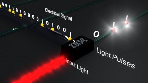
The new technology by IBM allows for electrical signals to combined with the light produced by a laser and create short pulses of light. These pulses can then be routed around the inside of a computer to transmit information at speeds much faster then our modern computers can accomplish today. Credit: ibmchips (Flickr Commons)
Second, a laser can be passed through specially designed optical logic gates, made from crystals with a non-linear refractory index, to perform arithmetic and logical operations within the computer’s processing unit at light speed.
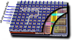
By utilizing specially manufacturing crystals, the new technology produced by IBM can create logic gates, the fundamental circuitry that makes decisions inside the CPU, that utilize light rather than the traditional electronic circuity. Not only does this have the benefit of fast-as-light speeds, but the circuitry operates cooler than the modern computer and utilizes far less electricity. Credit: Programmazione.it2010 (Flickr Commons)
In December of 2012, IBM announced that it had designed and created a hybrid silicon photonics-electronic chip, and not only that, but they also managed to integrate the monolithic manufacturing process used to make CPUs today.
This breakthrough by IBM in silicon photonics found two key benefits. First, there is the difference in performance. Where traditional CPUs are able to move data around the computer in the mere gigabytes per second, comparatively, tests on the new IBM photonics chip show the speed to be in the terabytes per second. From this capability, IBM has predicted that communication between computers, or between CPUs within a computer, could see a speed increase by a factor of one thousand. Second, because IBM was able to use a similar manufacturing process, that is not too different from the way CPUs are made today, this means that this technology could be offered commercially quickly, cheaply and integrate with current computer hardware almost seamlessly.
So what does this mean for the future of computation? Will silicon photonics contribute to the forthcoming revolution in computer manufacturing? Tell me what you think and stay tuned for part two when I look at developments in new materials that will shape the computers of the future.
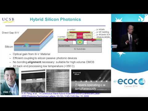
For a more detailed breakdown of the silicon photonics, check out the presentation given by the Director of the Institute for Energy Efficiency and Kavli Professor of Nanotechnology at the University of California Santa Barbara, John Bowers. Bower’s presentation at the 2014 European Conference on Optical Communications provides some of the finer details of this exciting new technology in the video below:
– Corey Wilson