Tag Archives: IBM

Moving Beyond Silicon (Part Two): The Unlimited Potential of Graphene

In Part One of this series, I discussed an overarching trend in computer science called Moore’s Law. This law (think of it as a law of computer nature) states that roughly every two years, the overall processing power of the conventional computer will double. Now, while this may be exciting to the consumer who cannot wait to get their hands on a faster computer for the same price; the consequences of this law for the computer engineers who create the devices, have never been more challenging.

The most difficult of these challenges is that as more components are put into the central processing unit (CPU) of a computer, the components will need to become so small that they will eventually reach the size of a single atom! Once at that hard limit, there will simply be no more room left in the microchip for more components. Consequently, the method of how we manufacture computers will need to be drastically reimagined if technological innovation is to continue in the foreseeable future.

Moore's Law and Technological Innovation

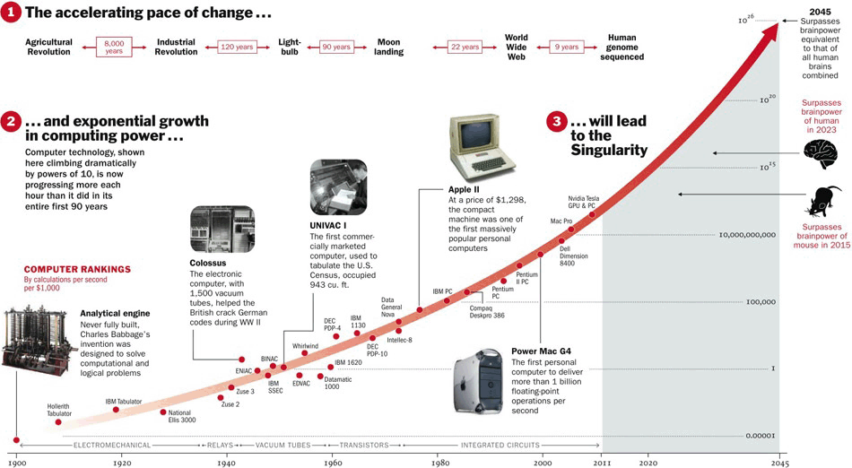
Moore’s Law can be directly linked to technological innovation. As our computers become more powerful, cutting-edge technologies proliferate. Credit: Humanswlord (WordPress)

That said, as many novel options for how to compute information differently have become available, scientists have wondered if the problem lies in what we compute our information with. Particularly, what if extending Moore’s Law for the next century meant that we only had to change the material we make our computers with? Enter the miracle material, graphene.

Put simply, graphene is a very thin layer of carbon, measuring only one atom thick. These single carbon atoms are packed together tightly to form what is known as a hexagonal honeycomb lattice.

Graphene in a Hexagonal Honeycomb Lattice

Graphene in a Hexagonal Honeycomb Lattice. Each carbon atom (represented by the “C”) is perfectly bonded to it’s neighbours. Credit: Karl Bednarik (Wikimedia Commons).

This unique structure of carbon atoms makes graphene the thinnest, lightest, strongest, best heat and electricity conducting material known to science. Not only that, but due to carbon being the fourth most abundant element in the universe, it could very well be the most sustainable material also.  However, it isn’t what graphene is that makes it so spectacular, but what it can do when put it to the task of computation.

In 2013, IBM showed their first generation of graphene-based integrated circuit (IC). Just this last year, IBM announced another breakthrough in creating its next generation of IC built with graphene. In this new generation of graphene based IC, IBM layered graphene in the channels of a microchip (the spots where electricity is conducted and electrons are moved around). From applying graphene in this way, IBM found the microchip to be 10,000 times faster then the current silicon alternative which uses copper. From this, IBM claims that graphene based electronics possess the potential to reach speeds upwards of 500ghz (that is 500 billion operations per second or 20 times faster then the conventional laptops sold today). This is made possible because graphene has little to no electrical resistance, which means it can move electrons around the processor much more efficiently then copper ever could.

With that said, there are still many hurdles which must be passed before graphene makes it into your next mobile device. For one, graphene based IC’s remain incredibly difficult to build using traditional processes for manufacturing microchips. IBM stated that current methods of creating graphene for use in IC’s remain expensive and inefficient. That said, it is only a matter of time before manufacturing processes are streamlined and the great graphene revolution in computer science begins!

For more information on graphene, check out this video by SciShow below.

YouTube Preview Image

Vive la graphene!

– Corey Wilson

Moving Beyond Silicon: Taking on Moore’s Law with Photonics

“It can’t go on forever. The nature of exponentials is that you push them out and eventually disaster happens”

This stark comment made in 2005 by Gordon E. Moore, a co-founder of Intel, has served as a wakeup call for computer scientists who have known for nearly forty years that mainstream manufacturing processes for computer circuitry will soon become obsolete.

Ever since its original conception in 1965, Moore’s Law has predicted that roughly every two years, the number of transistors put into a computers central processing unit (CPU) will double. Moreover, each time the amount of transistors doubles,  Why should you care about this trend? First, progress in the development of the increasingly intelligent technologies that effect our lives relies heavily on this trend. Insofar as over time, we depend on our computers becoming faster, while simultaneously staying cool, small and economic to operate; so that we can innovate with them.

PPTMooresLawai

Much of human progress, from consumer electronics to medical breakthroughs, relies on the Moore’s Law continuing for the foreseeable future. Credit: Ray Kurzweil and Kurzweil Technologies, Inc. (Wikimedia Commons)

Second, Intel has predicted that as soon as 2021, new strategies for designing computer hardware will need to be implemented or development of exciting new technologies will be stunted dramatically. Consequently, computer scientists have been researching the future of manufacturing the CPU, and the prospects are encouraging.

Optoelectronics_experiment

An electro-optics researcher experiments with routing lasers. Credit: Adelphi Lab Center (Wikimedia Commons)


Take for instance, silicon photonics, a development in CPU design that will allow signals to be processed within the computer using lasers which guide photons  rather than traditional electronic circuits which pass information using electrons. Silicon photonics develops computing in two key ways. First, a hybrid silicon laser can be used to encode information using pulses of light and pass the laser through guides to transmit information quickly to other parts of the computer.

2108713905_44d262678d_o

The new technology by IBM allows for electrical signals to combined with the light produced by a laser and create short pulses of light. These pulses can then be routed around the inside of a computer to transmit information at speeds much faster then our modern computers can accomplish today. Credit: ibmchips (Flickr Commons)


Second, a laser can be passed through specially designed optical logic gates, made from crystals with a non-linear refractory index, to perform arithmetic and logical operations within the computer’s processing unit at light speed.

5228755628_8a6e249b49_o

By utilizing specially manufacturing crystals, the new technology produced by IBM can create logic gates, the fundamental circuitry that makes decisions inside the CPU, that utilize light rather than the traditional electronic circuity. Not only does this have the benefit of fast-as-light speeds, but the circuitry operates cooler than the modern computer and utilizes far less electricity. Credit: Programmazione.it2010 (Flickr Commons)


In December of 2012, IBM announced that it had designed and created a hybrid silicon photonics-electronic chip, and not only that, but they also managed to integrate the monolithic manufacturing process used to make CPUs today.

This breakthrough by IBM in silicon photonics found two key benefits. First, there is the difference in performance. Where traditional CPUs are able to move data around the computer in the mere gigabytes per second, comparatively, tests on the new IBM photonics chip show the speed to be in the terabytes per second. From this capability, IBM has predicted that communication between computers, or between CPUs within a computer, could see a speed increase by a factor of one thousand. Second, because IBM was able to use a similar manufacturing process, that is not too different from the way CPUs are made today, this means that this technology could be offered commercially quickly, cheaply and integrate with current computer hardware almost seamlessly.

So what does this mean for the future of computation? Will silicon photonics contribute to the forthcoming revolution in computer manufacturing? Tell me what you think and stay tuned for part two when I look at developments in new materials that will shape the computers of the future.

For a more detailed breakdown of the silicon photonics, check out the presentation given by the Director of the Institute for Energy Efficiency and Kavli Professor of Nanotechnology at the University of California Santa Barbara, John Bowers. Bower’s presentation at the 2014 European Conference on Optical Communications provides some of the finer details of this exciting new technology in the video below:

YouTube Preview Image

– Corey Wilson